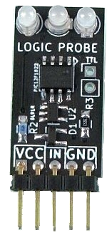
Breadboard Logic Probe
Breadboard Logic Probe
a breadboard friendly logic probe
that indicates logic HIGH, LOW, and PULSE.
Design Documents
| Schematic Diagram | schematic_J413A_breadboard_logic_probe.pdf |
| Bill of Materials | Breadboard Logic Probe BOM.pdf |
| PCB Gerbers | gerbers_J413A_breadboard_logic_probe.zip |
| Source Code | code_J413A_breadboard_logic_probe.zip |
Specifications
| Power Requirement | 3.3V to 5.0V, 25mA maximum |
| Input | TTL or CMOS levels, jumper selectable |
| Indicators | HIGH, LOW, PULSE |
Operation
The Logic Probe PCB is designed to plug into 5 rows of a standard breadboard.
picture
There are 5 breadboard pins, at least 3 of which must be connected
| 1) VCC 2) VCC | Logic supply voltage, 3.3V to 5.0V, connect to either power pin |
| 3) IN | Signal Input |
| 4) GND 5) GND | Logic ground, connect to either ground pin |
LED Indicators
| Left | Green | LOW |
| Middle | Yellow | PULSE |
| Right | Red | HIGH |

The "TTL" jumper determines what logic levels will be used
| No Jumper | CMOS logic levels |
| Jumper Installed | TTL levels |
